Our MProbe system measurement principle is based on spectroscopic reflectance and/or transmittance. Practically, any transluscent material coating or film can be measured.
MProbe systems are available in a wide wavelength range – from UV to IR; we select transparency window within this range. This means that even if material is totally opaque in the visible range (appears opaque to the eye), we still maybe able to measure it by using NIR or IR range. One example is thin film solar applications: absorbers (CIGS, CdTe, etc.) are specifically designed to absorb visible spectrum. Using the NIR wavelength range (900-1700nm) we are able to measure thickness of the absorbers without any problem. Surface roughness can also limit the ability to measure. Again, surface roughness effect increases dramatically at the shorter wavelength (UV and Vis) range – using NIR helps reduce its effect and makes measurement possible. Typically, films with surface roughness < 30nm can be measured using Visible system and with roughness <70nm with NIR system: in both case, actual roughness value can be determined as well.
Thickness range:
The thickness range is material dependent but, in general, from 1 nm to 1mm). Optical constants can be measured for thicknesses > 200nm (maybe thinner for absorbing material ). The thickness range is dependent on measurement wavelength range, spectrometer resolution and material refractive index.
Number of layers:
There is no limit on the number of layers. In most cases, we can accurately measure up to 5 layers (the filmstack itself can have any number of additional layers that are not measured). As the number of measured layers increases – precision of the measurement decreases. However, there are some exceptions:for example, optical coatings like interference filters or heterostructures (HEMT) that consist of repeated pair of layer (can be hundreds of layers). In this case, layers are not independent and our software allows to treat them as “linked” layers – hundreds of layers can be determined without problem.
Substrate
Substrate by definition is a material that has infinite thickness – this means that the light from the bottom interface of the substrate never comes back i.e. reaches detector. For example, Si wafer is a substrate in a visible range but a thin polymer or glass is not. If the substrate is very thin (e.g. 1 mm glass) it is treated as a special layer and backside reflectance is taken into account.
Metal layers
Very thin metal layers (typically <50nm) can be measured, but thicker layer are opaque and cannot be measured with optical technique.Check details of Metal Film measurable ranges
Filmstack information
Optical measurements are indirect. In order to determine parameters of the layers, one needs to create a model of the filmstack. Model includes number, type of layers, nominal thickness etc. If material properties are unknown, one can start with a similar “known” material. For example, knowing the type of the material: dielectrics or conducting polymer, etc. is enough to build a model. In general, the more information is available – the easier it is to build a correct model and determine the exact parameters.
Many typical filmstacks are included in the database and 500+ materials are in materials database. A wide range of parameterized matarials is supported. New materials can be imported and/or created.
STAY IN THE KNOW - Sign for our monthly Newsletter.
Learn about latest development, applications and promotions
We take your privacy very seriously and never share your information with anybody. The information is kept encrypted and secure. You will only receive our monthly newsletter and you can unsubscribe at any time. If you have any questions or concerns - please contact us.
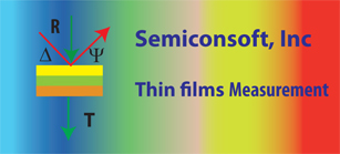
Thin film measurement system. Practically, any transluscent film can be measured quickly and reliably.
Everybody is an expert with MProbe